We will always do our best for a better product.
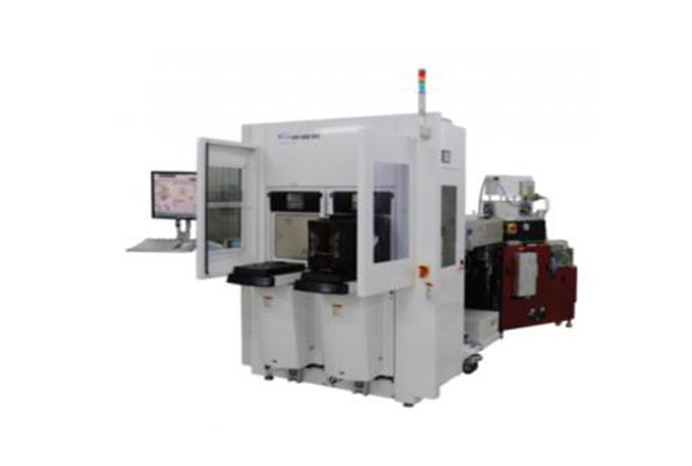
VSP-888 SW
Application
Descumming (PR, PI, PBO, BCB)
Surface reforming
Insulation film etching (SiO2, Si3N4)
Applying during bump forming used on wafer level packaging
Descumming sensitive film after development without damage to sensitive film of other area
for ensuring normal electroplating for bump forming

Specification
| Plasma source | ICP & RF bias |
|---|---|
| Wafer size | 200mm / 300mm |
| Wafer transfer | Vacuum transfer using loadLock |
| System dimension (mm) Process chamber |
2750 x 3130 x 1775 |
| Max 3 | |
| Application | Descum (PR, PI, PBO, BCB) |
| Surface modification | |
| Etch (SiO2, Si3N4) | |
| Operating software | Windows 7 |
| FIDES - cluster control software |
Features
-High etching uniformity: 〈 3%
-Brooks Platform with reliability demonstrated
-Oxidation preventing and particles reducing by conveyance in vacuum
-Applying optimized chamber for reducing dispensable costs
-Handling mold & class wafer by making use of high-capability ESC chuck